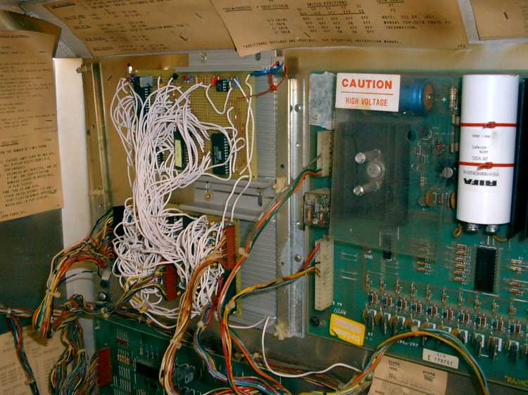
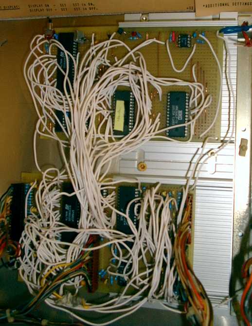
MPU prototype (based on Motorola 6809)
 After repairing some MPU boards for my pins,
I designed and built a MPU board from sratch with the following chips:
After repairing some MPU boards for my pins,
I designed and built a MPU board from sratch with the following chips:
6809 CPU
6264 Ram (or Zero Powerram)
27512 Rom
74hc21 and 74ls138 for adressdecoding
From the orginal board: 555,4049,4502, 4011, 2 * 6821
Hardware:
First goal find out the adressdecoding:
I created a memory map from original board:
    Chip Typ Adr.
    6810 Ram $0000-$007F
U10 6821 Pia $0088-$008b
U11 6821 Pia $0090-$0093
    5101 Ram $0200-$02ff (Warning: only the upper 4 bits are used !)
         Rom $1000-$1fff
         Rom $3000-$3fff
U6       Rom $5000-$5fff
U6       Rom $F000-$Ffff (duplicated)
The last rom is also mapped to $f000-$ffff, this is were the CPU takes out the start point.
Example: The harlemroms are used in the following way:
  Name       Adr.
l 750071.716 $1000
l 750082.716 $5000
l 720356.716 $5800
l 720356.716 $f800
(Same Information is found in pinmame)
Then I designed an adressdecoding with the two chips:
74ls138 and 72hc21.
With these chips I had three enable lines in sync with the clock signal:
One for the PIA's, one for the rom and one for the ram.
As input I used some adresslines from the CPU (A7,A9,A12) and the clock signal E.
So I get the folling new memmory map:
Roms $1000,$3000,$5000,$7000,$9000,$b000,$d000,$f000
Pias $008x (the pias have separate CSX lines)
Ram  $0200-$0FFF
Ram  $0000-$007f
The used adressdecodig is in detail described here:
http://www.izabella.freeuk.com/html/concluding_ideas.html
Second goal Clock circuit:
The 6809 has an integrated clock circuit, no need for an external clock circuit. Just take two caps and a crystal. The 6809 also generates a E signal which is similar to the signal 02.
This signal is used also for the adressdecoding. Details of the clock circuit is described in the motororla documentation which is still downloadable.
First I started with a crystal with 4 MHz . Then the board runs at 1 Mhz.
This was to quick for the Lamp driver board.
Now I'm working with a crystal with 2 MHz . Then the board runs at 500 khz.
(It should be 530 khz, thanks dave from allteksystem)
This seems to be the original speed. (see under problems)
Third goal easy reset circuit:
The reset circuit I made is quite easy. Because I don't want to use akku on the board for the ram I don't need a valid power detector. (I prefer Zeropowerram). I wired the LED direct to + 5 (I used a modern LED with a built in resistor for 5 V).
So i don't need + 12 on the board.
The rest of the schematic I leave. (Display interrupt, Zero Crossing detector, usw.)
Software:
I dissassembled the roms with dasmx.exe.
An easy start point for the codedection
are the Memory Vectors at the end of the ROM (FFFF-FFFE,...)
Because I got 6800 Code I did the folling modifications:
Include a Makro which maps the old 6800 instructions (inx) to 6809 instructions (lea X,1).
For the Dataareas I used org statments.
Then sometimes the mapping of the old 6800 instructions takes more place in the memory
and I had to move around some code. (but I have now plenty of space in the rom area).
I also assign the stack pointer to a new adress (LDS #$3ff), because the 6809 has some register
more which are stored by an interuppt on the stack.
The original Bally board uses only 4 Bits of the memory area $200-$2ff. The lower bits of this
memory area are always high. This means, if we have the folling piece of code:
     lda $#00
     sta $200
     lda $200

Then the A cointains $#0F !
I created a Marco AFF (which is nothing more than an ora #0b00001111) to simulate this behavior.
New Code:

    lda $#00
    sta $200
    lda $200
    aff

Now A cointains $#0F again.
Major Problems I had:
The Lamp board is adressed sequential (See Bally TOF for details,great book).
First the board was to quick, the lamps were not adressed correctly (they flicker only).
So I used a lower crystal and I have to add some wait statments in the Update Lamp section of the programm.
Then every lamp works, except the first four (1k, 2k ,3k , 4k).
The Lamp update section itself is placed in an interrupt routine which is also interruped by the
Display Update routine. This routine uses the same Adresslines (PA0-PA7) but the Lamp board
should only react if the Lamp Strobe Line goes from High to Low.
Then I load via software the Adress FFFF into the Lamp board before I started to update the Lamp board.
This solved the problem.
The other problems where easy:
1) I forget to add a resistor in the schema for the reset line, the CPU doesn't start.
2) I forget to add a resistor on the board for the IRQ line, the CPU boots all the time.
Schemas:
Part 1
Part 2
or as jpg
Part 1
Part 2
Mail me